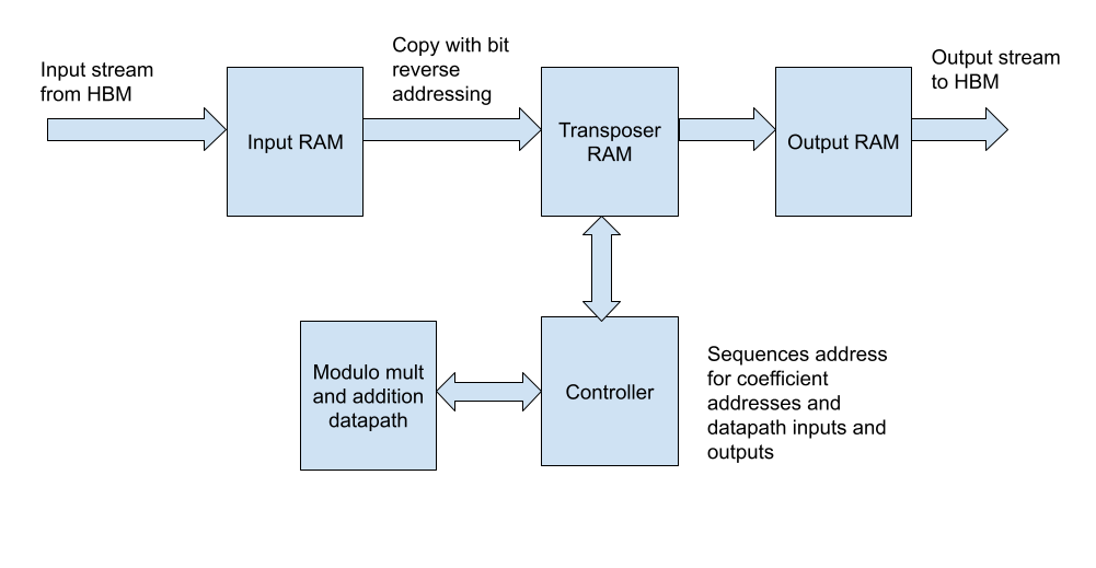
Data path
The data path consists of 2 field multipliers and adders.
The multipliers are used in the transform phase to process one full butterfly operation per cycle. This consists of scaling the input coefficient and also the root of unity. Thus the performance of this architecture is N/2 * log N.
The data path is reused to perform the twiddle phase after the first pass of the 4-step algorithm. Each coefficient must be scaled by a specific root of unity and then the root scaled. This pass take N cycles.
Controller
The controller sequences the address for coefficient RAMs and the controls the data path.
RAMs
We required 2 read and 2 write ports for all RAMs in the design. This includes the inputs RAMs, internal RAMs, and output RAMs.
Since FPGA RAMs consist of 2 ports, we build our require structure from 2 UltraRAMs. Each UltraRAM has both it's ports connected to either the read or write side.
When a flip signal is toggled the port directions swap.
The RAMs are architectued such that we can load new INNT coefficents, store a processed INTT, and perform a INNT in parallel.
Scaling
Our design can be parameterized by logcores and logblocks.
The Parallel_cores block instantiates 1 << logcores INTT blocks. It also defines the width of the data path into the cores.
The Multi_parallel_cores block instantiates 1 << logblocks Parallel_cores blocks. This the design scales with 1 << (logcores + logblocks) cores.
API Documentation
Documentation
