Implementation Details
Our implementation targets a AWS EC2 f1.2xlarge instance. This instance contains a single VU9P part. We have utilized the aws-fpga Vitis flow in our hardware design and the Xilinx Run Time (XRT) in our host code to interface with the FPGA.
High-Level Implementation Overview
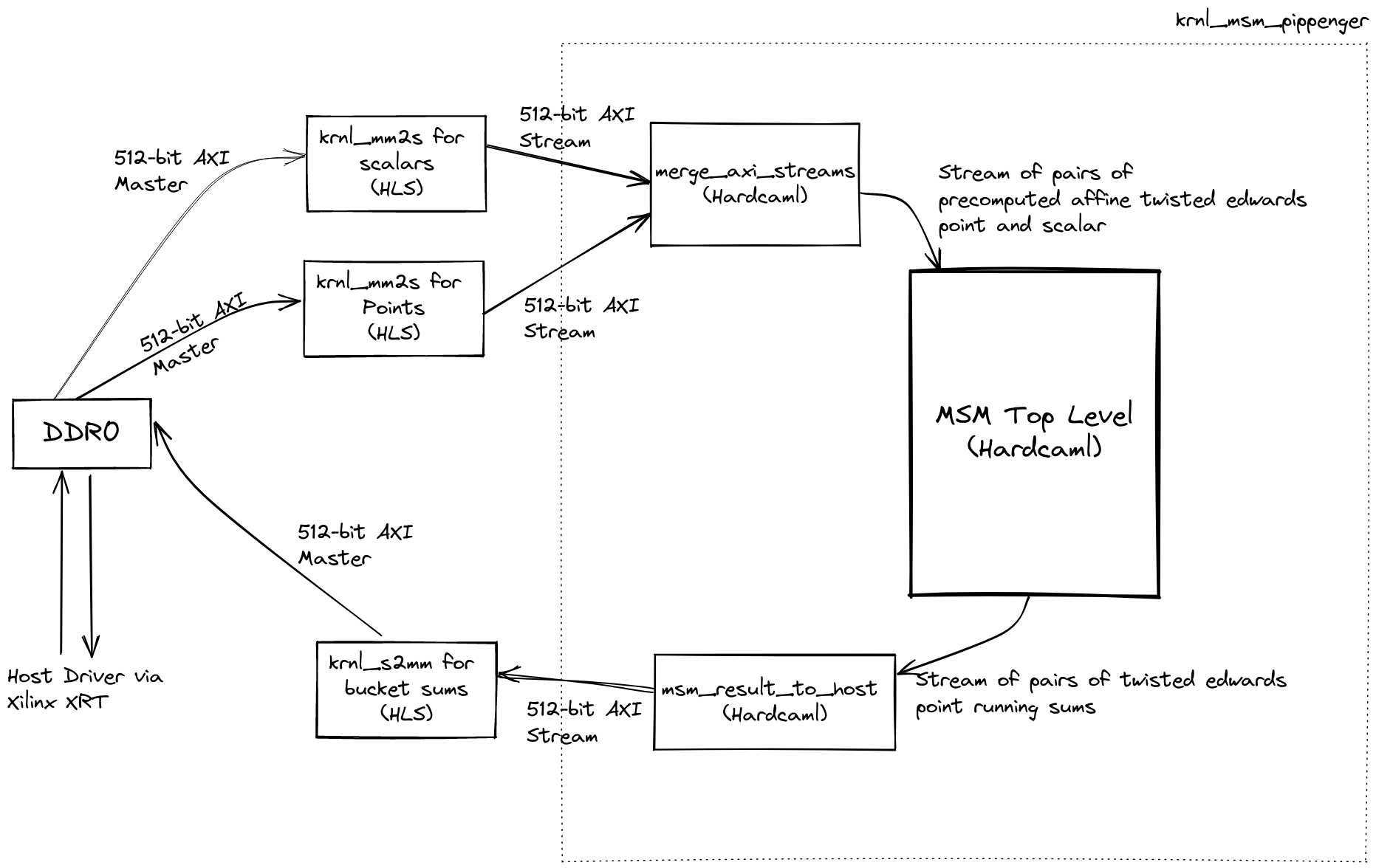
Our FPGA design comprises of the following 3 high-level components
- Memory Access Blocks (written with HLS)
- IO transformation blocks (written in Hardcaml)
- MSM block to compute pippenger bucket aggregation (written in Hardcaml, discussed in detail in other sections)
Memory Access Blocks
The memory access blocks (krnl_mm2s and krnl_s2mm) interface with a
DDR memory bank via an AXI interface and transform them to/from AXI
streams.
We have two separate HLS kernels loading affine points and scalars from DDR, and a single HLS kernel to write bucket values to DDR. Using HLS blocks for these simple tasks is a massive productivity boost:
- AXI Streams are much easier to work with than AXI ports in RTL
- The HLS kernels have a predefined API for communication with the host drivers
We used a single DDR bank for scalars, points and bucket values, because:
- Our memory access pattern is streaming friendly
- Our computation is nowhere near memory bound
- The AWS shell has only 1 memory controller built-in
We futher modify the memory access block krnl_mm2s to allow us to set the tlast bit of the
AXI stream when transfering data from the host. This was part of the key of allowing a subset of the point and scalar
inputs to be streamed from DDR into the FPGA, while performing other calculations on the host
in parallel.
IO Transformation Blocks
The memory access blocks read / write AXI streams with a bus width of 512-bits. We have some IO transformation blocks to reshape the stream into the appropriate data format.
The merge_axi_stream block converts the 512-bit AXI stream into a stream of
scalars and affine points and aligns the streams to be available at same clock cycle.
The msm_result_to_host block does a similar alignment on the bucket values
output to be written back to the host.
Engineering to Improve Performance
Targeting a High Frequency
At realistic frequencies, our design is compute bound, rather than memory bound. So increasing frequency directly results in a faster MSM.
The Vitis linker config file allows us to easily specify a target frequency to compile our design at. This makes it very convenient to experiment with targeting various clock frequencies with a simple config file change.
Another nice feature of the Vitis is that it automatically downclocks the design when it fails to meet timing closure. This allows us to experiment with high frequencies aggressively, and still have a working design after a long 12-hour build that fails timing. In our submission, we used a config that targets 280MHz, but got downclocked to 278MHz.
(Note that the choice of frequency might affect the implementation results! Notably, targeting 278MHz directly might not have delivered the same result.)
Vivado Implementation Strategies
We experimented with various Vivado implementation strategies. We found that
Congestion_SSI_spreadLogic_high tends to deliver better results, likely
due to the high congestion in our design.
Not Enabling Retiming
We have experimented with synthesis retiming by adding
set_param synth.elaboration.rodinMoreOptions "rt::set_parameter synRetiming true"
in our pre-synthesis hooks. Surprisingly, we have found that it degrades a
build’s frequency from ~250MHZ to ~125MHZ!. We did not investigate why. We
hypothesize that this could be due to the presence of a lot of
register->register paths in our design dedicated for SLR crossing which synth
retiming tries to insert combinational logic into, damaging routing results.
Needless to say, we did not include retiming as part of our submission!
SLR Partitioning
Modern FPGAs are really several dies stacked together with limited interconnect resources between them. Xilinx calls these dies Super Logic Regions (SLRs). The VU9P FPGA contains 3 SLRs. There are interconnects between SLR0<->SLR1 and SLR1<->SLR2.
In our design, we have carefully partitioned our design such that the RAM for running bucket values for the windows are carefully spreaded out into 3 SLRs, and the pipelined point adder’s various stages are explicitly splitted across multiple SLRs and fitted with necessary SLR-crossing registers.
Hardcaml makes some of these complicated partitioning choices a lot more manageable. We have config fields that allow us to specify the following:
- How the windows RAM should be partitioned – specifically, we can assign the number of windows per SLR.
- The assignment of adder stages to different SLRs. The design will dynamically instantiate necessary SLR crossing between stages as needed.
We added the following pre placement script to make the process of assigning
module instantiations to SLRs more convenient. With this simple configuration,
our Hardcaml design simply needs to add _SLR{0,1,2} suffix to instantiation
names based on the config to map a module instantiation into a particular SLR.
add_cells_to_pblock pblock_dynamic_SLR0 [get_cells -hierarchical *SLR0*]
add_cells_to_pblock pblock_dynamic_SLR1 [get_cells -hierarchical *SLR1*]
add_cells_to_pblock pblock_dynamic_SLR2 [get_cells -hierarchical *SLR2*]