Core (I)NTT design
The core NTT design (code documentation) performs transform of sizes which can fully fit within FPGA Block or UltraRAM resources. This limits us to transform sizes of around $2^16$.
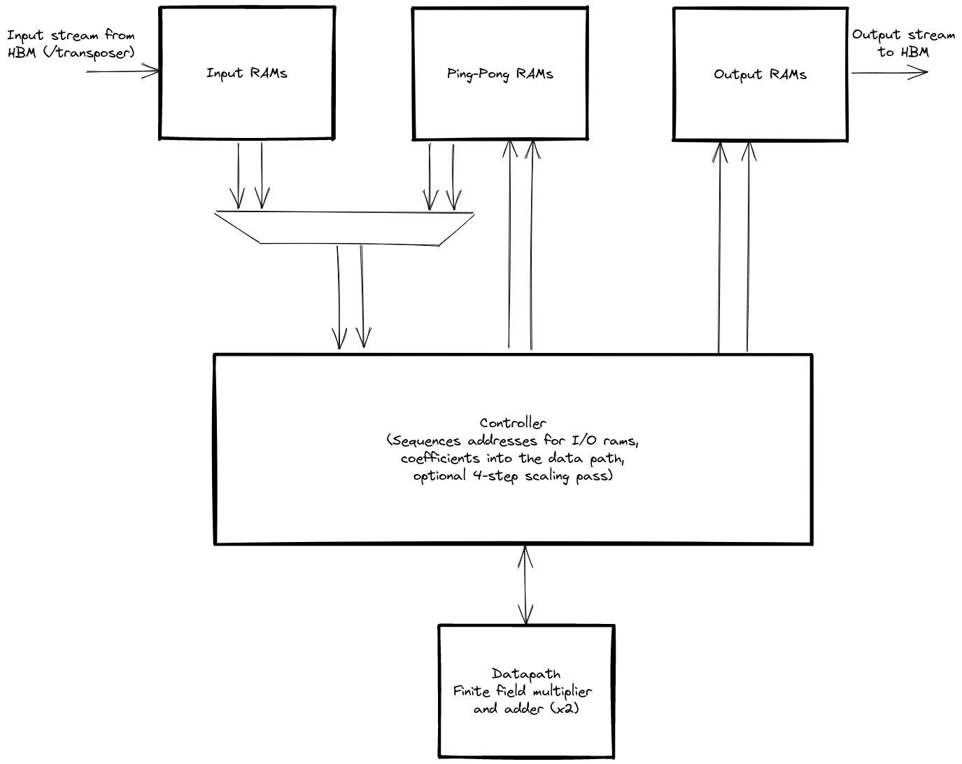
The general architecture of the core NTT is shown in the diagram below.
The core is designed to perform one butterfly operation per cycle. This involves two finite field multiplications per cycle (one for the butterfly operation and one to update the root of unity).
To keep the data path fully utilised we need to be able to read and write two coefficients per cycle. The various RAMs used to store coefficients are architected to allow two simultaneous read and write ports.
For a size-$N$ transform (note $N$ is assumed to be a power of 2) we require $log_{2}N$ iterations.
Since we perform a full butterfly operation per cycle we require a total of $N/2 log_{2}N$ cycles to perform the full transform.
The actual number of cycles is slightly larger than this. In order to achieve a clock rate of 250Mhz, the butterfly data path (including the finite field multiplier) must be pipelined. The pipelining is currently set at 8 clock cycles. After each NTT iteration we must account for datapath pipelining to ensure data integrity. At transform sizes greater than $2^8$ this extra cost becomes negligible.
Controller
The controller sequences a decimation in time NTT.
- Generates input and output addresses, including the required bit-reversal in the first iteration.
- Routes data to/from the appropriate RAM depending on the iteration.
- Synchronises RAM access with data pipelining after each iteration to ensure data integrity.
- Optionally controls the scaling step after the first pass in the full 4-step design.
Data path
The data path consists of 2 field multipliers and adders and takes and produces 2 coefficients per cycle.
The datapath is heavily pipelined, which is a problem for updating the root each cycle. To overcome this we implemented the twiddle factor stream module. This is initialised with the first few roots (in a small ROM) to hide the multiplier latency while producing a new root each cycle.
In the full design, the data path is reused to perform the twiddle phase after the first pass of the 4-step algorithm. Each coefficient must be scaled by a specific root of unity and then the root scaled. This pass takes a further N cycles and hides the multiplier latency using a trick similar to the one used by the twiddle factor stream module.
RAMs
We required 2 read and 2 write ports for all RAMs in the design. This includes the input RAMs, internal ping-pong RAMs, and output RAMs.
Since FPGA RAMs consist of 2 ports, we build the required structure from 2 UltraRAMs. Each UltraRAM has both its ports connected to either the read or write side.
When a flip signal is toggled the port directions swap.
The RAMs are architected such that we can load new NTT coefficients and store a processed NTT concurrently with an NTT computation.